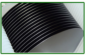
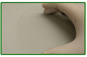
Diameter: 2”, 3”, 100 mm, 125 mm, 150 mm, 200 mm, 300 mm
Grade: Prime, Test, Monitor, Dummy, Reclaim
Growth: CZ, FZ
Type / Dopant: P/B, N/Ph, N/Sb, N/As, Undoped, Intrinsic (Only FZ)
Orientation: <100>, <111>, <111> 40 OFF, <110>
Resistivity: 0.001 – 50,000 ohm – cm
Thickness: 100 – 8,000 µm
Surface Finish: SSP, DSP, As Cut, As Lapped, Etched
Flat / Notch: SEMI Std., Single Flat, Jeida Flat, Notched, None (Round)
Diameter: 2”, 3”, 100 mm, 125 mm, 150 mm, 200 mm, 300 mm
Material: Borofloat, Fused Silica, Quartz Glass, BK7, Eagle XG, Soda Lime, B270
Thickness: ⩾ 200 µm
Surface Finish: DSP, As Lapped
Surface Quality: 20/10, 40/20, 60/40, 80/50
Surface Roughness: 6 – 10 Å
Diameter: 2”, 3”, 100 mm, 125 mm, 150 mm
Growth: Kyropolos, HEM
Purity: 99.99 – 99.998 %
Orientation: C- plane (0001), A- plane (11-20), R- plane (1-102), M- plane (10-10)
Surface Finish: Optical Polished, Epi-poloshed, Fine Ground, As Lapped
Surface Roughness: Polished: Ra<=0.3 nm, Fine Ground: <1 µm, As Lapped: <1 µm
Thickness: 430 ± 20, 460 ± 20, 625 ± 20
Size: 3” x 3”, 4” x 4”, 5” x 5”, 6” x 6”
Thickness: 0.04”, 0.09”, 0.25”, 1.5”
Material: Soda Lime, Quartz
Photoresist: AZ 1518, any custom resist, No Photoresist
Other Materials
Materials: GaAs, GaP, GaSb, InAs, InP, InSb, etc
Germanium
Diameter: 2”, 3”, 100 mm
Orientation: <1-0-0>, <1-1-1>
LiNbO3
Diameter: 2″, 3″, 100 mm, 150 mm
Orientation: Y-, Z-, YZ-, and OFF-Orientations
Single Crystal Quartz
Diameter: 2″, 3″, 100 mm, 150 mm
Orientation: Y-Cut, X-Cut, AT-Cut, ST-Cut


