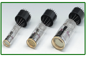
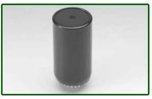
For Scintillation Counting, Fast Time Response Bialkali Photocathode, 8-stage, Head-on Type
Features:
- Fast Time Response
- Excellent Time Response
- Suitable for Mass Production
Specifications:
| Spectral Response | Maximum Rating | ||||||
| Range (nm) | Peak Wavelength | Photo cathode material | Window Material | Supply Voltage Between Anode & Cathode | Average Anode Current | ||
| 300 to 650 | 420 nm | Bialkali | Borosilicate glass | 1750 V | 0.1 mA | ||
| 300 to 650 | 420 nm | Bialkali | Borosilicate glass | 1750 V | 0.1 mA | ||
| 300 to 650 | 420 nm | Bialkali | Borosilicate glass | 1750 V | 0.1 mA | ||
| Cathode Characteristics | ||||||
| Dynode Structure/Stage | Anode to Cathode Supply Voltage |
Luminous | Blue Sensitivity Index (CS 5-58)Typ. |
Radiant Typ. |
||
| Min. | Typ. | |||||
| Linear-focused/8 | 1500 V | 70 µA/lm | 95 µA/lm | 10.0 | 80 mA/W | |
| Linear-focused/8 | 1500 V | 70 µA/lm | 95 µA/lm | 10.0 | 80 mA/W | |
| Linear-focused/8 | 1500 V | 70 µA/lm | 95 µA/lm | 10.0 | 88 mA/W | |
| Anode Characteristics | |||||||
| Luminous Typ. | Radiant Typ. | Gain Typ. | Dark Current(After 30 min.) | Time Response | |||
| Rise Time Typ. |
Transit Time Typ. |
Transit Time Spread |
|||||
| Typ. | Max. | ||||||
| 48 A/lm | 4.0 x 10 4 A/W | 5.0 x 10 5 | 3 nA | 30 nA | 0.9 ns | 10 ns | 170 ps |
| 48 A/lm | 4.0 x 10 4 A/W | 5.0 x 10 5 | 3 nA | 30 nA | 1.2 ns | 13 ns | 190 ps |
| 30 A/lm | 2.8 x 10 4 A/W | 3.2 x 10 5 | 10 nA | 50 nA | 2.0 ns | 20 ns | 270 ps |
Features:
- Flat response from visible to near IR minimizes spectral sensitivity correction.
- Photoluminescence from a room temperature sample can be measured.
- Time resolved measurement in near IR is realized.
Specifications:
General:
| Spectral Response | 300 to 1400 nm | 300 to 1700 nm | ||
| Photocathode | Material | InP / InGaAsP | InP / InGaAs | |
| Minimum Effective Area | 3 x 8 mm | |||
| Window | Material | Borosilicate glass | ||
| Dynode | Secondary Emitting Surface | Cu-BeO | ||
| Structure | Line focused | |||
| Number of Stage | 10 | |||
| Socket | C9940-01, -02 | |||
| Operating Temperature | -90 to -70 0C | |||
| Recommended Operating Temperature | -80 0C | |||
| Storage Temperature | -90 to +50 0C | |||
Characteristics (at -80 0C, Supply voltage: -1500 V)
| Min. | Typ. | Max. | Min. | Typ. | Max. | ||||
| CathodeSensitivity | Quantum Efficiency | 0.48 % | – | – | 0.29 % | – | – | ||
| Radiant | 5 mA/W | – | – | 3.5 mA/W | – | – | |||
| Anode Sensitivity | Radiant | 1000 A/W | – | – | 700 A/W | – | – | ||
| Gain | 2 x 10⁵ | 1 x 10⁶ | – | 2 x 10⁵ | 1 x 10⁶ | – | |||
| Anode Dark Current | – | 4 nA | 10 nA | – | 40 nA | 100 nA | |||
| Anode Dark Counts | – | 1.6 x 10⁴ s-1 | – | – | 1.6 x 10⁵ s-1 | – | |||
| TimeResponse | Anode Pulse Rise Time | – | 3 ns | – | – | 3 ns | – | ||
| Electron Transit Time | – | 23 ns | – | – | 23 ns | – | |||
| Transit Time Spread | – | 1.5 ns | – | – | 1.5 ns | ||||
Features:
- High Speed
- Rise Time: 170 ps (Typ.)
- IRF (Instrument Response Function): ≤ 70 ps (FWHM) (Typ.)
Specifications:
- General:
| Spectral Response | 950 to 1400 nm | 950 to 1700 nm |
| Wavelength of Peak Response | 1300 nm | 1500 nm |
| Photocathode Material | InP / InGaAsP | InP / InGaAs |
| Window Material | Borosilicate Glass | |
| Effective Area of PMT | Ø 2 mm | |
| Stage of MCP | 2 stages Filmed MCP | |
| Operating Ambient Temperature | -90 to -70 0C | |
| Storage Temperature | -90 to +50 0C | |
- Maximum Rating:
| PMT Supply Voltage | -3400 V | |
| Average PMT Anode Current | 20 nA | |
- Characteristics (at -3000 V, -80 0C)
Min. Typ. Max. Min. Typ. Max. CathodeSensitivity Quantum Efficiency 0.1 % 1.0 % – 0.1 % 1.0 % – Radiant 1.0 mA/W 11 mA/W – 1.2 mA/W 12 mA/W – Gain 1 x 10⁵ 3 x 10⁵ – 1 x 10⁵ 3 x 10⁵ – Anode Dark Current – 2 x 10⁴ s-1 1 x 10⁵ s-1 – 5 x 10⁴ s-1 2.5 x 10⁵ s-1 Voltage Driver Current – – 110 µA – – 110 µA TimeResponse Rise Time – 170 ps – – 170 ps – Fall Time – 700 ps – – 700 ps – IRF – 70 ps 100 ps – 70 ps 100 ps
Specifications:
- General:
| Spectral Response | 950 to 1400 nm | 950 to 1700 nm |
| Wavelength of Peak Response | 1300 nm | 1500 nm |
| Photocathode Material | InP / InGaAsP | InP / InGaAs |
| Window Material | Borosilicate Glass | |
| Effective Area of PMT | Ø 2 mm | |
| Stage of MCP | 2 stages Filmed MCP | |
| Operating Ambient Temperature | -90 to -70 0C | |
| Storage Temperature | -90 to +50 0C | |
- Maximum Rating:
| PMT Supply Voltage | -3400 V | |
| Average PMT Anode Current | 20 nA | |
- Characteristics (at -3000 V, -80 0C)
| Parameter | Min. | Typ. | Max. | Min. | Typ. | Max. | ||
| CathodeSensitivity | Quantum Efficiency | 0.1 % | 1.0 % | – | 0.1 % | 1.0 % | – | |
| Radiant | 1.0 mA/W | 11 mA/W | – | 1.2 mA/W | 12 mA/W | – | ||
| Gain | 1 x 10⁵ | 3 x 10⁵ | – | 1 x 10⁵ | 3 x 10⁵ | – | ||
| Anode Dark Current | – | 2 x 10⁴ s-1 | 1 x 10⁵ s-1 | – | 5 x 10⁴ s-1 | 2.5 x 10⁵ s-1 | ||
| Voltage Driver Current | – | – | 110 µA | – | – | 110 µA | ||
| TimeResponse | Rise Time | – | 170 ps | – | – | 170 ps | – | |
| Fall Time | – | 700 ps | – | – | 700 ps | – | ||
| IRF | – | 70 ps | 100 ps | – | 70 ps | 100 ps | ||
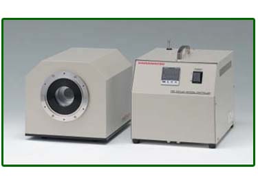
- Cooler:
| Input Voltage | AC 230 V, 50 Hz | ||
| Coolant Medium | Liquid Nitrogen (LN2) | ||
| Temperature Controllable Range | -70 to -90 0C (Continuously adjustable) | ||
| Cool-down Time | About 2 h (-80 0C setting) | ||
| Liquid Nitrogen Consumption | Approx. 0.5 L/h | ||
| Holder | -HV Connector | SHV-R | |
| Signal Connector | SMA-R | ||
| Load Resistor | Open | ||
| Power Consumption | 60 VA | ||
| Operating Ambient Temperature | +10 to +40 0C | ||
| Weight | Cooling Unit | Approx. 6 Kg | |
| Controller, etc. | Approx. 11 Kg | ||
| System Configuration | Cooling Unit, Controller, Control Cable, Silicon Tube, Insulated Transfer Hose, LN2 Transfer Head | ||
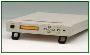
Bench-top type multipurpose power supply incorporating a high voltage power supply (maximum output of -2000V for photomultiplier tube).
Specifications:
| Type | Bench top type |
| Input Voltage | AC 100 to 240 V |
| Max. Output Voltage | -2000 V |
| Max. Output Current | 1.8 mA |
| Guaranteed Output Voltage Range | -320 to -2000 (variable) V |
| Line Regulation | ± 0.05 (for 10 % change in line voltage) % |
| Load Regulation | ± 0.03 (For 0 % to 100 % change in load)% |
| Ripple/Noise | 0.003 * (*Unit:%) mV |
| Temperature Coefficient | ± 0.01 % / 0C |
| Operating Ambient Temperature | 0 to +40 0C |
| Operating Ambient Humidity | Below 85 % |
| Storage Temperature | -20 to +50 0C |
| Storage Humidity | Below 90 % |
| Power Consumption | 60 VA |
| Dimensions | 246 mm x 85 mm x 312 mm |
| Weight | Approx. 3.0 Kg |
Product Variation:
| Spectral Response | Features |
| 185 nm to 750 nm | High sensitivity in UV to Visible range |
| 185 nm to 900 nm | For general applications in UV to near IR range |
| 185 nm to 900 nm | High sensitivity in UV to near IR range |
| 185 nm to 830 nm | Low dark current in UV to near IR range |
| 185 nm to 650 nm | For general application in UV to visible range |
Specifications:
| Parameter | ||||||||||
| -01 | -02 | -03 | -04 | -05 | ||||||
| Input Voltage | +11.5 to +15.5 V | |||||||||
| Max. Input voltage | +18 V | |||||||||
| Max. Input Current | 7 mA | |||||||||
| Max. Output Signal Current | 10 µA | |||||||||
| Max. Control Voltage | +1.2 (Input impedance: 1Ω) | |||||||||
| Recommended control voltage adjustment range | +0.25 to +1.0 V | |||||||||
| Effective Area | 3.7 x 13.0 mm | |||||||||
| Peak Sensitivity Wavelength | 420 nm | 400 nm | 450 nm | 530 nm | 340 nm | |||||
| Cathode | Luminous Sensitivity | Min. | 80 µA/lm | 200 µA/lm | 350 µA/lm | 140 µA/lm | 20 µA/lm | |||
| Typ. | 120 µA/lm | 300 µA/lm | 500 µA/lm | 200 µA/lm | 40 µA/lm | |||||
| Blue Sensitivity Index | Typ. | 10 | – | – | – | 5 | ||||
| Red/White Ratio | Typ. | – | 0.3 | 0.4 | 0.15 | – | ||||
| Radiant Sensitivity | Typ. | 90 mA/W | 77 mA/W | 105 mA/W | 70 mA/W | 48 mA/W | ||||
| Anode | Luminous Sensitivity | Min. | 100 A/lm | 400 A/lm | 1000 A/lm | 300 A/lm | 50 A/lm | |||
| Typ. | 700 A/lm | 1200 A/lm | 2000 A/lm | 700 A/lm | 300 A/lm | |||||
| Radiant Sensitivity | Typ. | 5.2 x 10⁵ A/W | 3.1 x 10⁵ A/W | 4.2 x 10⁵ A/W | 2.5 x 10⁵ A/W | 3.6 x 10⁵ A/W | ||||
| Dark Current | Typ. | 1 nA | 1 nA | 2 nA | 0.1 nA | 0.5 nA | ||||
| Max. | 10 nA | 10 nA | 10 nA | 1 nA | 5 nA | |||||
| Rise Time | Typ. | 1.4 ns | ||||||||
| Ripple Noise (Peak to peak) | Max. | 0.5 mV | ||||||||
| Setting Time | Max. | 10 s | ||||||||
| Operating Ambient Temperature | +5 to +50 0C | |||||||||
| Storage Temperature | -20 to +50 0C | |||||||||
| Weight | 110 g | |||||||||
| Anode | Luminous Sensitivity | Min. | 100 A/lm | 400 A/lm | 1000 A/lm | 300 A/lm | 50 A/lm | |
| Typ. | 700 A/lm | 1200 A/lm | 2000 A/lm | 700 A/lm | 300 A/lm | |||
| Radiant Sensitivity | Typ. | 5.2 x 10⁵ A/W | 3.1 x 10⁵ A/W | 4.2 x 10⁵ A/W | 2.5 x 10⁵ A/W | 3.6 x 10⁵ A/W | ||
| Dark Current | Typ. | 1 nA | 1 nA | 2 nA | 0.1 nA | 0.5 nA | ||
| Max. | 10 nA | 10 nA | 10 nA | 1 nA | 5 nA | |||
| Rise Time | Typ. | 1.4 ns | ||||||
| Ripple Noise (Peak to peak) | Max. | 0.5 mV | ||||||
| Setting Time | Max. | 10 s | ||||||
| Operating Ambient Temperature | +5 to +50 0C | |||||||
| Storage Temperature | -20 to +50 0C | |||||||
| Weight | 110 g | |||||||
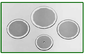
Circular MCP:
MCP (Microchannel Plate) is a two-dimensional sensor that detects electrons, ions, vacuum UV rays, X-rays and gamma rays, and amplifies the detected signals.
Specifications:
| Outer size | Ø 38.4 mm | Ø 86.7 mm | Ø 113.9 mm |
| Electrode Area | Ø 36.5 mm | Ø 84.7 mm | Ø 112 mm |
| Effective Area | Ø 32 mm | Ø 77 mm | Ø 105 mm |
| Thickness | 0.48 mm | 1 mm | 1 mm |
| Channel Diameter | 12 µm | 25 µm | 25 µm |
| Channel Pitch | 15 µm | 31 µm | 31 µm |
| Bias Angle θ | 8 degrees | 8 degrees | 8 degrees |
| Open Area Ratio | 60 % | 60 % | 60 % |
| Electrode Material | Inconel | Inconel | Inconel |
| Gain (Min.) | 104 | 104 | 104 |
| Resistance | 20 to 100 MΩ | 10 to 100 MΩ | 5 to 50 MΩ |
| Dark Current (Max.) | 0.5 pA.cm2 | 0.5 pA.cm2 | 0.5 pA.cm2 |
| Max. Linear Output | 7 % o Strip Current | 7 % o Strip Current | 7 % o Strip Current |
| Supply Voltage | 1.0 kV | 1.0 kV | 1.0 kV |
| Operating Ambient Temp. | -50 to +70 0C | -50 to +70 0C | -50 to +70 0C |
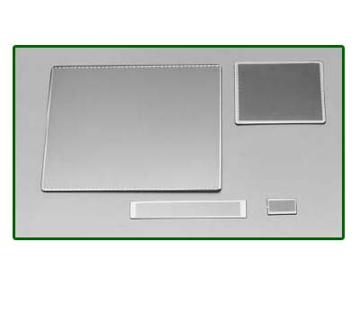
Rectangular MCP:
Specifications:
| Outer size | 15.9 x 9.4 mm | 49.9 x 39.9 mm | 59.9 x 59.9 mm | 96.9 x 96.9 mm |
| Electrode Area | 15 x 8.5 mm | 49 x 39 mm | 58 x 58 mm | 95.6 x 77.3 mm |
| Effective Area | 13 x 6.5 mm | 45 x 35 mm | 53 x 53 mm | 90 x 72 mm |
| Thickness | 0.48 mm | 0.48 mm | 0.80 mm | 1.00 mm |
| Channel Diameter | 12 µm | 12 µm | 20 µm | 25 µm |
| Channel Pitch | 15 µm | 15 µm | 25 µm | 31 µm |
| Bias Angle θ | 8 degrees | 8 degrees | 8 degrees | 8 degrees |
| Open Area Ratio | 60 % | 60 % | 60 % | 60 % |
| Electrode Material | Inconel | Inconel | Inconel | Inconel |
| Gain (Min.) | 104 | 104 | 104 | 104 |
| Resistance | 100 to 500 MΩ | 20 to 200 MΩ | 20 to 120 MΩ | 10 to 50 MΩ |
| Dark Current (Max.) | 0.5 pA.cm2 | 0.5 pA.cm2 | 0.5 pA.cm2 | 0.5 pA.cm2 |
| Max. Linear Output | 7 % o Strip Current | 7 % o Strip Current | 7 % o Strip Current | 7 % o Strip Current |
| Supply Voltage | 1.0 kV | 1.0 kV | 1.0 kV | 1.0 kV |
| Operating Ambient Temp. | -50 to +70 0C | -50 to +70 0C | -50 to +70 0C | -50 to +70 0C |
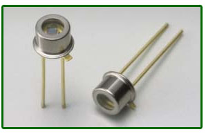
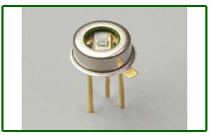
For High Power UV monitor, and UV to Visible, Precision Photometry
Features:
- TO-18 package with UV glass window
- High sensitivity from UV to near infrared range
- High reliability versus high power UV radiation
Applications:
- Mercury lamp (λ = 254 nm) monitor
- Excimer laser (KrF: λ = 248 nm) monitor
- Other UV detection
Si APD is a low bias, high speed APD for 900 nm wavelength. Si APD is designed to provide a peak sensitivity wavelength in the 900 nm band where optical rangefinders are increasingly used.
Features
– Peak sensitivity wavelength: 840 nm (gain=100)
– Low bias operation: Breakdown voltage=200 V max.
– High-speed response: Cutoff frequency=650 MHz typ.
Specifications:
| Type | High-speed type (for 900 nm, Low bias operation) |
| Photosensitive area | φ0.2 mm |
| Package | Metal |
| Package Category | TO-18 |
| Peak sensitivity wavelength (typ.) | 840 nm |
| Spectral response range (min.) | 400 to 1150 nm |
| Photosensitivity (typ.) | 0.52 A/W |
| Dark current (max.) | 1 nA |
| Cutoff frequency (typ.) | 650 MHz |
| Terminal capacitance (typ.) | 0.5 pF |
| Breakdown voltage (typ.) | 160 V |
| Temperature coefficient of breakdown voltage (typ.) | 1.1 V/℃ |
| Gain (typ.) | 100 |
Specifications:
| Window material | UV glass | UV glass | ||||||
| Package | TO-18 | TO-18 | ||||||
| Active area size | 1.1 x 1.1 mm | 1.1 x 1.1 mm | ||||||
| Effective active area | 1.2 mm2 | 1.2 mm2 | ||||||
| Reverse Voltage VR Max. | 5 V | 5 V | ||||||
| Operating Temperature Topr | -40 to +100 0C | -40 to +100 0C | ||||||
| Storage Temperature Tstg | -50 to +125 0C | -50 to +125 0C | ||||||
| Spectral Response Range λ | 190 to 1000 nm | 190 to 1100 nm | ||||||
| Peak Sensitivity Wavelength λp | 720 nm | 960 nm | ||||||
| Photosensitivity S | λp | 0.36 A/W | 0.50 A/W | |||||
| 200 nm | Min. | 0.06 A/W | 0.06 A/W | |||||
| Typ. | 0.075 A/W | 0.075 A/W | ||||||
| Short circuit Current100 lx | Isc | Min. | 0.5 µA | 1.0 µA | ||||
| Typ. | 0.66 µA | 1.2 µA | ||||||
| Dark Current ID VR=10 mV | Max. | 2 pA | 20 pA | |||||
| Temp. coefficient of | TCID | ID | 1.12 times/ 0C | 1.15 times/ 0C | ||||
| Rise time tr VR= 0, | RL=1kΩ | 0.15 µs | 0.1 µs | |||||
| Terminal capacitance CtVR= 0, f= 10 kHz | 35 pF | 20 pF | ||||||
| Shunt resistance Rsh | VR= 10mV | Min. 5 GΩ | Min. 0.5 GΩ | |||||
| Typ. 50 GΩ | Typ. 2 GΩ | |||||||

